
Author Affiliations
Abstract
1 State Key Laboratory on Integrated Optoelectronics, Institute of Semiconductors, Chinese Academy of Sciences, Beijing 100083, China
2 National–Local Joint Engineering Laboratory of New Energy Photovoltaic Devices, Key Laboratory of Digital Medical Engineering of Hebei Province, College of Electron and Information Engineering, Hebei University, Baoding 071002, China
3 College of Materials Science and Opto-Electronic Technology, University of Chinese Academy of Sciences, Beijing 100049, China
New neuromorphic architectures and memory technologies with low power consumption, scalability and high-speed are in the spotlight due to the von Neumann bottleneck and limitations of Moore's law. The memristor, a two-terminal synaptic device, shows powerful capabilities in neuromorphic computing and information storage applications. Active materials with high defect migration speed and low defect migration barrier are highly promising for high-performance memristors. Halide perovskite (HP) materials with point defects (such as gaps, vacancies, and inversions) have strong application potential in memristors. In this article, we review recent advances on HP memristors with exceptional performances. First, the working mechanisms of memristors are described. Then, the structures and properties of HPs are explained. Both electrical and photonic HP-based memristors are overviewed and discussed. Different fabrication methods of HP memristor devices and arrays are described and compared. Finally, the challenges in integrating HP memristors with complementary metal oxide semiconductors (CMOS) are briefly discussed. This review can assist in developing HP memristors for the next-generation information technology.
Journal of Semiconductors
2020, 41(5): 051205
长春理工大学光电工程学院, 吉林 长春 130022
针对制冷型中波红外640×512焦平面阵列探测器,设计了一个30×连续变焦光学系统,提出从前固定组中分离出1片透镜作为两档移动组,并与变倍组、补偿组及后固定组组合成复合连续变焦系统的设计方案。针对该模型,基于衍射光学理论设计了工作波段为3.7~4.8 μm,F数为4,可以实现12~360 mm连续变焦,光学总长仅有160 mm的制冷型中波红外连续变焦光学系统。给出了系统在6个焦距位置的像质情况,并对凸轮曲线进行优化设计。该系统具有高变倍比、结构小型化、像质优良、凸轮曲线平滑等优点,可以满足红外热成像仪的要求。
光学设计 中波红外 复合连续变焦 小型化

Author Affiliations
Abstract
1 State Key Laboratory on Integrated Optoelectronics, Institute of Semiconductors, Chinese Academy of Sciences, Beijing 100083, China
2 School of Electrical and Information Engineering, Tianjin University, Tianjin 300072, China
3 School of Microelectronics, Tianjin University, Tianjin 300072, China
Bipolar phototransistors have higher optical responsivity than photodiodes and play an important role in the field of photoelectric conversion. Two-dimensional materials offer a good optical responsivity and have the potential advantages of heterogeneous integration, but mass-production is difficult. In this study, a bipolar phototransistor is presented based on a vertical Au/graphene/ van der Waals heterojunction that can be mass-produced with a silicon semiconductor process using a simple photolithography process. Au is used as the emitter, which is a functional material used not just for the electrodes, is used for the collector, and graphene in used for the base of the bipolar phototransistor. In the bipolar phototransistor, the electric field of the dipole formed by the Au and graphene contact is in the same direction as the external electric field and thus enhances the photocurrent, and a maximum photocurrent gain of 18 is demonstrated. A mechanism for enhancing the photocurrent of the graphene/ photodiode by contacting Au with graphene is also described. Additionally, the maximum responsivity is calculated to be 16,458 A/W, and the generation speed of the photocurrent is A/s.
Photonics Research
2020, 8(1): 01000039
1 中国科学院大学微电子学院, 北京 100049
2 中国科学院大学材料与光电研究中心, 北京 100049
3 中国科学院半导体研究所集成光电子学国家重点实验室, 北京 100083
针对速率为100 Mbit/s、偏置电流为0.15 A的使用开关键控调制的可见光通信系统,通过软件仿真和实验验证相结合的方法,研究了调制度对通信系统性能以及照明效果的影响。结果表明,随着调制度的增大,误码率减小,且距离越短,误码率对调制度的变化越敏感。当速率为100 Mbit/s、距离为12.0 m时,在1 W荧光型发光二极管的可见光通信系统中,调制度最小为0.1就可以满足前向纠错误码率门限要求。如果对通信系统的可靠性要求较高,调制度应在0.1和误码率为0所对应的调制度之间选择,且调制度的大小不会对照明效果产生影响。
光通信 可见光通信 调制度 误码率
1 中国科学院半导体研究所 集成光电子学国家重点实验室, 北京 100083
2 中国科学院大学, 北京 100049
3 中国科学院脑科学与智能技术卓越创新中心, 上海 200000
为了减小神经电极的宽度, 提高电极在光照下的抗噪声干扰能力, 提出了一种基于0.18μm CMOS工艺的抗光噪声神经微电极。采用CMOS的多层布线代替传统电极导线的单层排布, 并将电极衬底接地以有效减小光噪声。阐述了基于CMOS工艺的神经电极结构设计、制备过程与结构表征, 并对所制备的神经电极进行了电化学阻抗测试和光噪声测试。该神经电极宽度仅为70μm, 实验证明: 1kHz频率下电极的阻抗一致性好, 且在1mW/mm2的光遗传常用光辐照下, 该电极的噪声电压仅为0.07~0.08mV, 远低于传统硅电极12~13mV的噪声幅值。结果表明, 基于CMOS工艺的神经电极抗光噪声能力远优于传统硅电极, 对硅基微电极在光遗传中的应用具有重要意义。
CMOS工艺 神经微电极 光噪声 电极宽度 CMOS process neural microelectrode light noise electrode width
Author Affiliations
Abstract
1 Key Laboratory of Optoelectronics Technology, Beijing University of Technology, Beijing 100124, China
2 State Key Laboratory of Integrated Optoelectronics, Institute of Semiconductors, Chinese Academy of Sciences, Beijing 100083, China
3 Department of Microtechnology and Nanoscience, Chalmers University of Technology, Gothenburg 41296, Sweden
4 e-mail: xieyiyang@bjut.edu.cn
5 e-mail: xuchen58@bjut.edu.cn
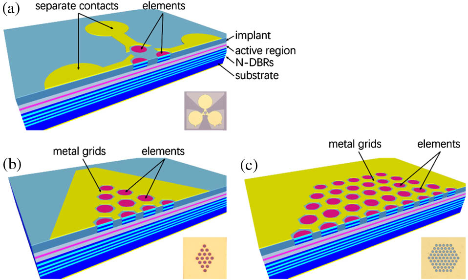
Optical coupling behavior and associated effects in two-dimensional implant-defined coherently coupled vertical-cavity surface-emitting laser (VCSEL) arrays are studied via both experiments and theoretical calculations. Experiments show that optical coupling between array elements can enhance the array’s output power. Additionally, optical coupling via leaky optical fields can provide extra optical gain for the array elements, which can then reduce the thresholds of these elements. Elements can even be pumped without current injection to emit light by receiving a strong leaky optical field from other array elements. Optical coupling can also cause unusual phenomena: the central elements in large-area coherently coupled VCSEL arrays that lase prior to the outer elements when the arrays are biased, or the average injection current required for each element to lase, which is much lower than the threshold for a single VCSEL. Theoretical calculations are performed to explain the experimental results.
Photonics Research
2018, 6(11): 11001048
1 北京工业大学 电子信息与控制工程学院 光电子技术教育部重点实验室, 北京 100124
2 中国科学院半导体研究所, 北京 100083
在光子晶体垂直腔面发射激光器中采用质子注入工艺, 使台面工艺变成纯平面工艺, 降低了光子晶体结构制备难度, 简化了器件制备, 提高了器件的均匀性。质子注入型光子晶体垂直腔面发射激光器中的光子晶体结构, 在电流限制孔小于光子晶体缺陷孔时, 仍能控制器件光束及模式特性, 该结果可用于优化器件阈值电流, 制备高性能低阈值电流基横模器件。实验所设计制备的器件, 在注入电流小于12.5 mA时, 阈值电流2.1 mA, 出光功率大于1 mW, 远场发射角小于7°, 有效验证了光子晶体结构在质子注入型面发射激光器中的光束改善及模式控制作用。
质子注入 光子晶体 垂直腔面发射激光器 proton-implanted photonic crystal VCSEL 红外与激光工程
2016, 45(12): 1205001
1 中国科学院大学, 北京 100049
2 中国科学院上海技术物理研究所, 上海 200083
3 中国科学院红外探测与成像技术重点实验室, 上海 200083
为提升一种新型交叉簧片柔性微位移机构的动力学性能, 采用响应曲面优化分析对微位移结构参数进行多目标优化设计。首先建立机构的FEA参数化模型, 分析机构的工作原理, 利用ANSYS对微位移机构进行动力学分析; 确定微位移机构的性能指标参数; 采用内切中心复合设计法建立响应曲面模型, 确定优化设计参数; 以交叉铰链簧片厚度作为优化设计变量, 前三阶频率作为目标函数, 微位移刚度作为约束函数, 采用非线性二次规划算法建立多目标参数优化模型, 在优化推荐的三个最优解中进行修正, 得到最终的设计方案。比较优化前后微位移机构的性能指标, 在机构刚度不变的情况下, 一阶频率提升80%, 二、三阶频率提升4%。研究得出以下结论, 簧片厚度对微位移机构动力学性能影响呈正相关, 且不同节点处簧片厚度影响不同, 采用该优化设计方案有效提升了机构的动力学性能。
交叉簧片柔性铰链 响应曲面 内切中心复合设计 非线性二次规划算法 优化设计 cross-spring pivot response surface methodology inscribed central composite designs NLPQL optimization design 红外与激光工程
2016, 45(10): 1018005
中国科学院半导体研究所 集成光电子学国家重点实验室, 北京 100083
研究了高速可见光通信(VLC)系统中荧光型LED光源的直流偏置电流大小与系统响应时间、误码率的关系; 搭建了高速可见光通信测试系统, 用于验证如何通过设置合适的LED光源的直流偏置电流使可见光通信系统达到更高的通信速率和更低的误码率。实验测试结果表明, 在直流偏置电流为60~80mA, 1W的荧光型LED的响应时间较短, 系统的误码率较低, 此时可见光通信系统可达到最大传输速率。
可见光通信 荧光型LED 直流偏置 误码率 visible light communication phosphorescent white LEDs DC bias BET
Author Affiliations
Abstract
1 State Key Laboratory of Integrated Optoelectronics, Institute of Semiconductors, Chinese Academy of Sciences, Beijing 100083, China
2 School of Computer and Communication Engineering, University of Science and Technology Beijing, Beijing 100083, China
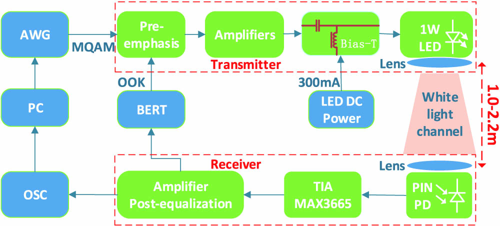
We experimentally demonstrate a high-speed phosphorescent white light emitting diode (LED) visible light communication (VLC) system without utilizing an optical blue filter. Here, the white light response is equalized by using the proposed analog equalizers. The 3 dB bandwidth of the VLC link could be extended from 3 to 132 MHz, which allows 330 Mbit/s non-return-to-zero on–off keying (NRZ-OOK) data transmission with a bit error ratio (BER) of 7.2×10 10 and 672 Mbit/s 64-quadrature amplitude modulation (64-QAM) data transmission with a BER of 3.2×10 3. These resultant BERs are less than the forward error correction (FEC) limit of 3.8×10 3. The VLC link distance is 1 m using a single 1 W LED. The transmitter and receiver modules are integrated to a compact size. Furthermore, the relationships between the signal performance and illumination level or optical power are investigated and analyzed.
060.4510 Optical communications 060.2605 Free-space optical communication 200.2605 Free-space optical communication Chinese Optics Letters
2015, 13(8): 080605


